Semiconductor Wafer and Chip Inspection Equipment
Maintaining yield in semiconductor production depends heavily on how early defects, contamination, alignment issues, and thermal instability are identified. From incoming wafer checks to package-level visual verification, Semiconductor Wafer and Chip Inspection Equipment supports critical control points across fabrication, assembly, and failure analysis workflows.
This category brings together inspection and support systems used to examine wafers, chips, and related processes with greater consistency and traceability. It covers both direct inspection platforms and enabling equipment such as chillers and thermal control devices that help stabilize measurement conditions during sensitive testing and imaging tasks.

Why inspection equipment matters in semiconductor processes
Semiconductor manufacturing tolerances are extremely tight, so even small scratches, particles, pattern deviations, or thermal drift can affect electrical performance and downstream yield. Inspection systems help engineering and quality teams detect issues earlier, document defect location, and compare process conditions over time.
Depending on the stage of production, the inspection objective may be different. Some applications focus on wafer surface defects and contamination, while others are aimed at package appearance, dimensional metrology, ESD-related evaluation, or non-destructive material analysis. For broader test workflows, users may also review related solutions in Semiconductor IC Testing Equipment when electrical characterization and inspection need to work together.
Typical equipment included in this category
This category is not limited to one machine type. It includes optical and metrology platforms for wafer and chip evaluation, automated systems for image-based defect detection, and supporting temperature control equipment used around inspection or test environments.
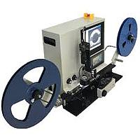
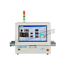
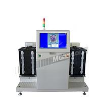
Examples from this range include the Nordson SQ3000M2 automated optical inspection and metrology system for high-resolution visual inspection, as well as SPIROX platforms such as the MA6500 Macro Inspection System and MA6503D Micro Inspection System for wafer surface review. For material and defect analysis, the SPIROX SP3055A non-destructive inspection system and SP8000A laser scanning confocal measurement development platform illustrate how this category can extend beyond standard visual checks into more advanced measurement tasks.
Inspection methods used for wafers and chips
Optical inspection remains one of the most common approaches because it supports fast screening of visible defects, foreign material, scratches, discoloration, alignment conditions, and surface anomalies. Systems in this group may combine cameras, controlled illumination, automated image processing, and software review tools to improve repeatability compared with manual inspection.
For more demanding analysis, manufacturers may need macro and micro inspection at different scales. Macro systems are useful for broader wafer-level review and defect mapping, while micro inspection can provide finer detail for defect classification, coordinate tracking, and image documentation. In some use cases, 3D or confocal measurement is added to evaluate height, coplanarity, surface topography, or localized structure changes that are harder to confirm with 2D imaging alone.
Role of temperature control in inspection stability
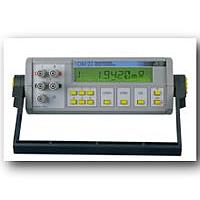
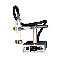
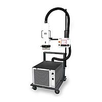
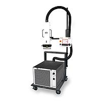
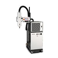
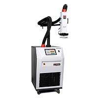
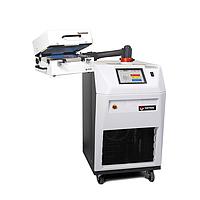
Inspection quality is not determined only by optics and software. In semiconductor environments, temperature stability can influence both the device under test and the measurement setup. Chillers and external circulators are often used to control process temperature, support thermal fixtures, or stabilize equipment operating conditions where repeatable results are important.
TAITEC models such as the CL-81, CL-151, and CL-601 show how open-circuit chiller solutions can cover different cooling capacities and control accuracy levels. For applications requiring a wider circulation temperature range, TAITEC CH-402N and CH-602N cooling pumps, as well as the DaiHan DH.Chi0020 refrigerated external circulator/chiller, help illustrate the supporting thermal infrastructure often needed around semiconductor inspection and evaluation systems. If your workflow is strongly centered on temperature conditioning, it may also be useful to compare options within semiconductor thermal test systems.
Representative manufacturers and solution ecosystems
Several established suppliers appear in this category, each with strengths in different parts of the inspection workflow. SPIROX is relevant for wafer inspection, confocal measurement, ESD-related equipment, and non-destructive analysis platforms used in semiconductor applications. Nordson is well known in optical inspection and metrology environments where automated visual quality control is part of packaging and assembly operations.
TAITEC and DaiHan add important process-support capability through chiller and circulation equipment, which can be highly relevant when thermal consistency affects measurement reliability. The overall result is a category that supports not only defect detection itself, but also the surrounding conditions required to keep inspection repeatable and production-friendly.
How to choose the right system
The best selection usually starts with the inspection target. Wafer-level review, chip/package inspection, incoming quality control, process monitoring, and failure analysis all require different imaging scale, motion accuracy, throughput, and software capability. Teams should define whether they need simple pass/fail screening, defect image storage, coordinate traceability, dimensional measurement, or more advanced surface characterization.
It is also important to check wafer size compatibility, defect size expectations, required field of view, and whether the process calls for 2D imaging, 3D inspection, or confocal measurement. If thermal effects are part of the application, circulation range and control stability should be reviewed alongside the inspection platform itself. For adjacent process needs, users comparing package-level manufacturing lines may also want to explore semiconductor packaging equipment.
Applications across production, quality, and engineering
These systems are used in incoming inspection, in-process control, outgoing quality assurance, and engineering analysis. In wafer workflows, they help identify contamination, scratches, crystal-related defects, and process irregularities before costly downstream steps continue. In assembly and packaging, automated optical inspection helps reduce reliance on manual visual checks and improves documentation of repeat defects.
Some platforms also support development and diagnostic work, especially when engineers need image records, defect coordinates, review software, or surface measurement data to correlate with process changes. Where ESD robustness or specialized test behavior must be studied together with inspection findings, categories such as SMU semiconductor test can provide additional context for electrical analysis workflows.
Finding the right fit for your inspection workflow
A practical inspection setup often combines more than one tool: automated optical inspection for speed, micro-level review for defect confirmation, and temperature control equipment for stable operating conditions. The right choice depends on product type, defect mechanism, required throughput, and how inspection data will be used by quality and process teams.
This category is designed to support those different scenarios with equipment spanning wafer inspection, chip and package review, metrology-oriented analysis, ESD-related systems, and thermal support. By matching the inspection method to the actual process risk, buyers can build a more consistent and traceable semiconductor quality workflow.
Get exclusive volume discounts, bulk pricing updates, and new product alerts delivered directly to your inbox.
By subscribing, you agree to our Terms of Service and Privacy Policy.
Direct access to our certified experts