
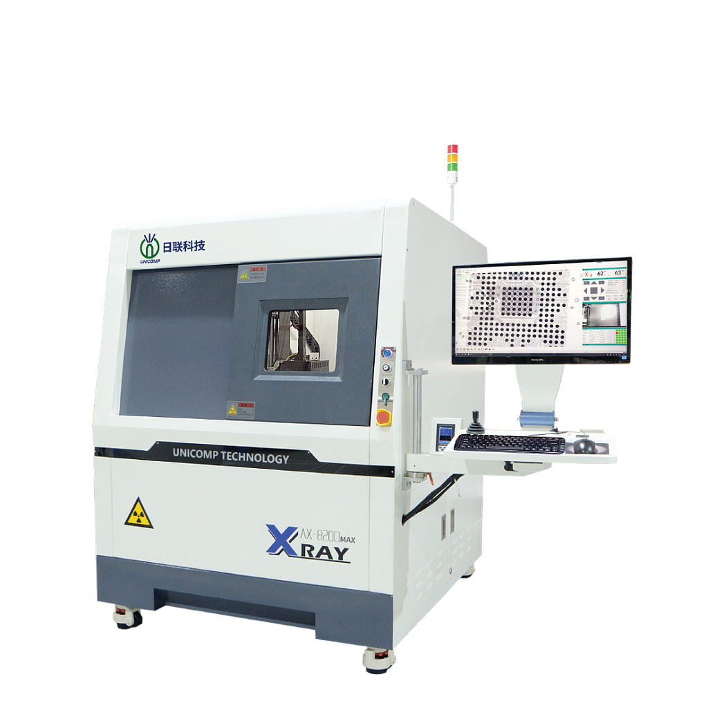
Unicomp AX8200MAX X-ray X-ray Inspection Equipment
AX8200 MAX
Size (L-W-H): 1350x1400x1700mm
Weight: 1350kg
Voltage: AC110-220V VAC50-60Hz
Maximum detection size: 570x550mm
Safety (radiation amount): <1uSv/h
Maximum sample weight: 10kg
Stage size: 580x550mm
X, Y, X axis distance: Light pipe Z axis 150, detector Z axis 290
As a new generation of upgraded and optimized AX8200, it can easily respond to the comprehensive and multi-angle product testing needs of different users.
Product description:
● Beautiful appearance design, equipped with large stage and desktop detection area
● The imager can perform 60° rotation and tilt detection and non-destructive magnification
● Small opening angle ray source also realizes 60° high-definition real-time imaging
● CNC programming running detection and matching with 24-inch full-display touch screen operation interface
● Powerful image analysis and measurement tools, automatically measure the bubble void ratio of solder joints
● Rotary lifting console integrates newly developed information verification safety identification and ray energy monitoring system
Application areas:
Used in semiconductor, SMT, DIP, electronic component testing, covering IC, BGA, CSP, flip chip and other package types testing, and can also be used in automotive parts, aluminum die-casting molds, LEDs, batteries, photovoltaic industries and molding Special industry testing such as plastic and ceramic products.
Detection images:

Get exclusive volume discounts, bulk pricing updates, and new product alerts delivered directly to your inbox.
By subscribing, you agree to our Terms of Service and Privacy Policy.
Direct access to our certified experts