
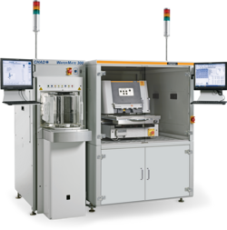
FISCHER FISCHERSCOPE X-RAY XDV-MUE SEMI 膜厚計
Fully automated wafer handling and testing boost efficiency
XRF system with excellent detector sensitivity and high resolution
XRF system with polycapillary optics from the worldwide technology leader for measuring micro-spots
Accurately tests structures up to 10 µm in diameter
Automatic pattern recognition pinpoints the positions to be measured
Multiple operating modes; manual measurement possible whenever required
Flexible: docking station for FOUP, SMIF and cassette, for 6", 8" and 12" wafers
Applications
- Coating Thickness Measurement:
Base metallization layers (UBM) at the nanometer scale
Thin lead-free solder caps on copper pillars
Extremely small contact surfaces and other complex 2.5D / 3D packaging applications
- Material Analysis:
C4 and smaller solder bumps
Lead-free solder caps on copper pillars
Brochure
数量割引、まとめ買い価格の更新、新製品情報をメールでお届けします。
登録することで、当社の利用規約およびプライバシーポリシーに同意したものとみなされます。
認定専門家へ直接アクセス