
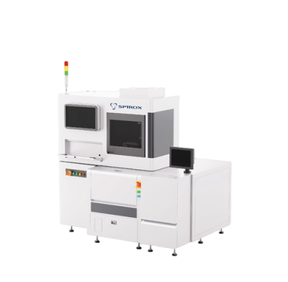
SPIROX MA6503D マイクロ検査システム (300μm ~ 2000μm, 8- and 12-inch wafer)
Function
Replace QC visual inspection on surface defects
Auto-storing wafer surface defects image and position coordinate records
Wafer
Compatible with 8-inch and 12-inch Wafer
Wafer Thickness: 300μm ~ 2000μm
Wafer Handling
Support automatic opening function for 12-inch FOUP cassette
Wafer ID Scan
Pre-aligner (Notch Location)
Chuck
Support wafer leveling function
Stage Flatness < 15μm
X/Y Axis Accuracy: ±1.7μm
Wafer Alignment
Optical
Camera: Line scan camera with 3x lens
FOV: Scanning length of 24mm x 300mm
2D Image Inspection
Minimum Defect Size: 5μm (Gray > 30)
Discoloration Inspection
Scratches Inspection
Contamination Inspection
Process Defects Inspection
Support PMI (Probe Mark Inspection) Scan Function
3D Image Inspection
Z-axis Resolution: 5μm
Measurement of Bump height and coplanarity (Ball High Limit: 800μm)
Software
Compatible with Wafer ID OCR
Output Format: .bmp or .jpg
Online Review System
Defect Image Output Format: SINF File
Optional
Offline Review System
Customized Report
Feature:
Utilize a Line Scan Camera with wide FOV and fast scanning capabilities
Use a 3x lens to enhance image quality and improve the defect characteristics inspection
5μm Defects Inspection Items: Particles, Scratches, Pad Defects, Bump Defects
Support Probe Mark Inspection (PMI) and offer PAD quick selection for detection settings
Support 3D inspection to measurement of Bump height and coplanarity
Auto wafer-level chuck with ±1.7μm accuracy to process high accuracy wafer coordinate alignment
Zoning parameter setting to realize accurate inspection requirement by zones
数量割引、まとめ買い価格の更新、新製品情報をメールでお届けします。
登録することで、当社の利用規約およびプライバシーポリシーに同意したものとみなされます。
認定専門家へ直接アクセス