
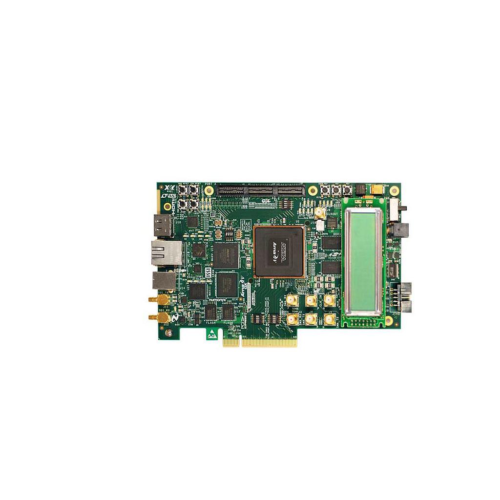
Terasic Altera Arria V GX Starter Kit
FPGA:
Arria V GX 5AGXFB3H4F35C4N
System controller: MAX® V 5M2210ZF256C4N
Power monitor GUI
Single analog-to-digital converter (ADC), eight channels
Non-isolated power rail
Fast passive parallel (FPP) x16 mode through parallel flash loader (PFL)
Control and status registers
Embedded USB-BlasterTM II:
MAX II EPM570GM100C4N
HDMI 1.3 TX
x4 XCVR, 2.7 Gbps (max by level shifter) and 270 MHz TX clock HDMI TX connector
STMicroelectronics HDMI level shifter STHDLS101T
Level shift XCVR PCML 1.5V <-> TMDS level
DDC and HPD <-> HDMI compliant level
Data channel up to 2.7 Gbps; HDMI 1.3 compliant
Clock channel up to 270 MHz; enough to support 2.7 Gbps data rate
HDMI specification: clock period = 10x of UI
SDI 3G
x1 XCVR TX/RX loopback
x2 SMB connectors and cable (cable not included in kit)
Up to 2.97 Gbps
Uses National Semiconductor driver/receiver LMH0384SQ/LMH0303SQx
Requires 148.5 MHz and 148.35 MHz at XCVR refclk to support US and EU standard respectively
Use VCXO to fine tune and lock to the recovered CDR frequency
HSMC
x8 XCVR up to 6.375 Gbps
Not complied to PCI Express® (PCIe® ) HIP pin assignment
x4 CMOS
x8 TX and x9 RX differential interface using dedicated TX/RX channels
x2 low-voltage differential signalling (LVDS) clock in
x2 differential clock out
I2C
JTAG
Minimum current support
2A @ 3.3V
1A @ 12V
Dedicated clock domain from Si 5338 clock generator for xcvr refclk
HSMC loopback with BTS GUI
SMA
1x XCVR TX/RX channel
1x LVPECL clock input
1X LVPECL clock output
Clocking
Dedicated clock domain from Si 5338 clock generator for xcvr refclk
DDR3 SDRAM x32
Micron MT41J64M16LA-15E DDR3 SDRAM 8MX16X8
Two devices: 2 x16 width = x32
BTS DDR3 SDRAM GUI using Uniphy and high performance (HP) controller II
SSRAM
512k x36, 18 Mb ISSI IS61VPS51236A
Shared address or data with flash
User IO
LCD character
x4 DIP switch
x3 PB
x4 LED
Configuration
FPP x16 mode
Dual flash 512Mbit Numonyx PC28F512P30BF (52 MHz FMAX )
JTAG header
Embedded USB Blaster II
Cypress Microcontroller CY7C68013A as USB PHY 2.0
MAX II
Ethernet
10/100/1000 Base-T
RJ-45 connector, on-board LED for link status
Marvell Ethernet PHY 88E1111
Requires 50 MHz clock from CLKIN
The Altera® Arria® V GX Starter Kit provides a complete design environment that includes all the hardware and software you need to develop cost-sensitive FPGA applications immediately. The development kit is RoHS compliant. The development kit features the following:
- Arria V GX FPGA—360KLE, F1152 package, 24X6.5G XCVRs, C4 speed grade
- One I/O expansion slot—one high-speed mezzanine card (HSMC) connector
- 256 MB of SDRAM memory
- High-definition multimedia interface (HDMI) and serial digital interface (SDI) connections
- SMAs
Đăng ký nhận chiết khấu độc quyền, cập nhật giá sỉ và tin sản phẩm mới nhất ngay tại hộp thư của bạn.
Bằng cách đăng ký, bạn đồng ý với Điều khoản dịch vụ và Chính sách bảo mật của chúng tôi.
Kết nối trực tiếp với đội ngũ chuyên gia của chúng tôi