
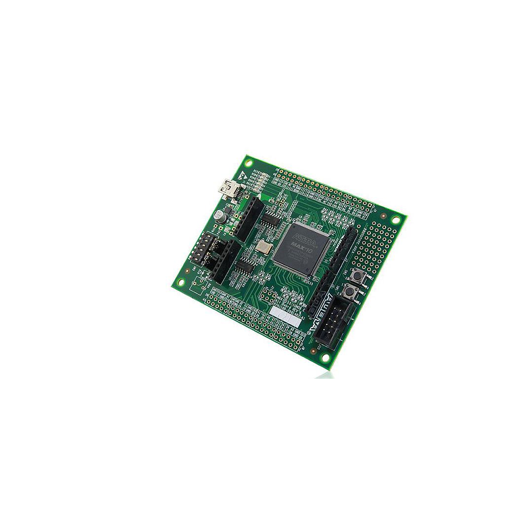
Terasic Altera MAX 10 FPGA Evaluation Kit
Altera MAX 10 FPGA, 10M08SAE144C8G, (or ES variant)
8,000 logic elements (LE)
378 kilobits (Kb) M9K memory
32 – 172 (KB) user flash memory
One analog-to-digital (ADC) converter, 1 million samples per second (MSPS), 12-bit
FPGA configuration circuitry
JTAG header for external USB-Blaster™, USB-Blaster II, or Ethernet Blaster download cable
Flash storage for two configuration images (factory and user)
Dual-image self-configuration via Programmer Object File (.pof)
Temporary engineering debug of FPGA design via SRAM Object File (.sof)
On-Board clocking circuitry
50 MHz oscillator connected to FPGA global clock input
General user I/O
8 analog input I/O, 14 Arduino I/O, 40 general purpose I/O
5 red user-defined LEDs
One green LED to show power from USB cable
Push button and DIP switches
One reconfiguration push button (SW2)
One device-wide reset of all registers, push button (SW1)
User DIP switch (SW3)
Power
The board is powered by USB cable (from PC or wall jack)
One green power-on LED (D6)
Probe points for manual, multi-meter measurement of current to calculate
Power consumption (TP2 - TP5) or to verify voltages on the selected internal nodes (TP1, TP6 - TP9)
The 10M08 evaluation board will enable a cost effective entry point to MAX 10 FPGA design. The card comes complete with Arduino header socket, which will enable a wide variety of daughter cards to be connected.
- 10M08SAE144C8G
- Arduino shield expansion
- Access to 80 I/O through-holes
- Prototype area
Đăng ký nhận chiết khấu độc quyền, cập nhật giá sỉ và tin sản phẩm mới nhất ngay tại hộp thư của bạn.
Bằng cách đăng ký, bạn đồng ý với Điều khoản dịch vụ và Chính sách bảo mật của chúng tôi.
Kết nối trực tiếp với đội ngũ chuyên gia của chúng tôi