
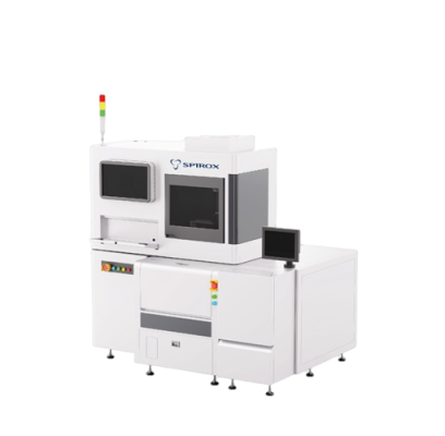
SPIROX MA6503D Micro Inspection System (300μm ~ 2000μm, 8- and 12-inch wafer)
Function
Replace QC visual inspection on surface defects
Auto-storing wafer surface defects image and position coordinate records
Wafer
Compatible with 8-inch and 12-inch Wafer
Wafer Thickness: 300μm ~ 2000μm
Wafer Handling
Support automatic opening function for 12-inch FOUP cassette
Wafer ID Scan
Pre-aligner (Notch Location)
Chuck
Support wafer leveling function
Stage Flatness < 15μm
X/Y Axis Accuracy: ±1.7μm
Wafer Alignment
Optical
Camera: Line scan camera with 3x lens
FOV: Scanning length of 24mm x 300mm
2D Image Inspection
Minimum Defect Size: 5μm (Gray > 30)
Discoloration Inspection
Scratches Inspection
Contamination Inspection
Process Defects Inspection
Support PMI (Probe Mark Inspection) Scan Function
3D Image Inspection
Z-axis Resolution: 5μm
Measurement of Bump height and coplanarity (Ball High Limit: 800μm)
Software
Compatible with Wafer ID OCR
Output Format: .bmp or .jpg
Online Review System
Defect Image Output Format: SINF File
Optional
Offline Review System
Customized Report
Feature:
Utilize a Line Scan Camera with wide FOV and fast scanning capabilities
Use a 3x lens to enhance image quality and improve the defect characteristics inspection
5μm Defects Inspection Items: Particles, Scratches, Pad Defects, Bump Defects
Support Probe Mark Inspection (PMI) and offer PAD quick selection for detection settings
Support 3D inspection to measurement of Bump height and coplanarity
Auto wafer-level chuck with ±1.7μm accuracy to process high accuracy wafer coordinate alignment
Zoning parameter setting to realize accurate inspection requirement by zones
Get exclusive volume discounts, bulk pricing updates, and new product alerts delivered directly to your inbox.
By subscribing, you agree to our Terms of Service and Privacy Policy.
Direct access to our certified experts