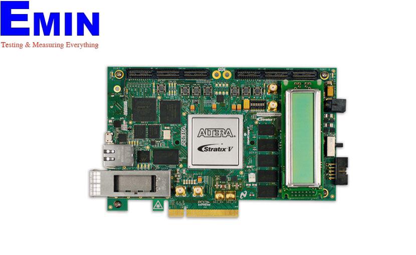
Terasic Altera Stratix V GX FPGA開発キット
生産者: Terasic Model: Altera Stratix V GX FPGA - 要件クオート

- 要件クオート
- 連絡先
1. Featured device:
Stratix V GX FPGA: 5SGXEA7K2F40C2N
2. Configuration, status, and setup elements
JTAG
On-board USB-BlasterTM II cable
Fast passive parallel (FPP) configuration via MAX® V device and flash memory
One reset config push button
One CPU reset push button
Two configuration push buttons
3. Clocks
50-MHz, 125-MHz, 100-MHz, and 148.5-MHz programmable oscillators
SMA input (LVPECL)
4. General user input and output
10/100/1000Mbps Ethernet PHY (SGMII) with RJ-45 (copper) connector
16x2 character LCD
One 8-position dual in-line package (DIP) switch
Sixteen user LEDs
Three user push buttons
5. Memory devices
DDR3 SDRAM (1,152 MB, x72-bit wide)
QDR II+ SRAM (4.5 MB, 2-Mb x18-bit wide)
Footprint compatible to QDR II 4-Mb x18-bit wide
RLDRAM II (72-Mbyte CIO RLDRAM II with an 18-bit data bus)
6. Component and interfaces
PCIe x8 edge connector
Two HSMC connectors
SMB for serial digital interface (SDI) input and output
QSFP optical cage
10/100/1000Mbps Ethernet PHY (SGMII) with RJ-45 (copper) connector
7. Power
Laptop DC input
PCIe edge connector
Nios® II processor web server and remote system update
The Altera® Stratix® V GX FPGA Development Kit provides a complete design environment that includes all the hardware and software you need to begin developing FPGA designs immediately. The development kit is RoHS compliant. You can use this development kit to do the following:
- Develop and test PCI Express® (PCIe®) designs at data rates up to Gen3 using the PCIe short card form factor-compliant development board
- Develop and test memory subsystems for DDR3, QDR II+, or RLDRAM II memories
- Use the high-speed mezzanine card (HSMC) connectors to interface to one of over 35 different HSMCs provided by Altera partners, supporting protocols such as Serial RapidIO®, 10-Gbps Ethernet, SONET, CPRI, OBSAI, and others
- 良質な取り決め
- オリジナル保証
- 宅配便
- 買い取り簡単化