
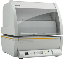
FISCHER FISCHERSCOPE X-RAY XDV-µ PCB 코팅 두께 측정기 (Ø 20 µm halofree*)
Universal instrument for automated measurements on smallest structures, multilayers, functional coatings and very thin coatings < 0.1 µm
Microfocus tube with tungsten anode; molybdenum anode optional
Measuring direction with measuring top down
4-fold changeable filters
Polycapillary optics permit particularly small measuring spots Ø approx. 20 or 10 µm
Silicon drift detector 20 or 50 mm² for highest precision on thin layers
Programmable measuring table for printed circuit boards up to 613 × 610 mm, optionally with vacuum function
Applications
Au/Pd/Ni/CuFe and Sn/Ni coatings in the micro- and nanometer range
Assembled and unassembled circuit boards
Testing of base metallization layers (under-bump metallization, UBM) in the nanometer range
Measurement of light elements, e.g. determination of the phosphorus content (in ENEIG/ENEPIG) under Au and Pd
Lead-free solder caps on copper pillars
Testing the elemental composition of C4 and smaller solder bumps, as well as small contact surfaces in the semiconductor industry
Brochure
인증된 전문가에게 직접 연결