빠른 지원
인증된 전문가에게 직접 연결
인증된 전문가에게 직접 연결
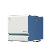
Function
Replace IQC visual inspection on surface defects (Including particles, scratches, etc.)
Auto-storing wafer surface defects image and position coordinate records
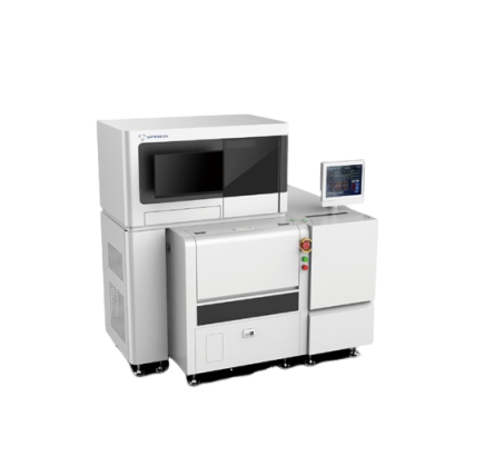
Wafer
Compatible with 8-inch and 12-inch wafer
Wafer Thickness: 300μm ~ 2000μm
Wafer Handling
Support automatic opening function for 12-inch FOUP cassette
Wafer ID Scan
Pre-aligner (Notch Location)
Optical
Camera: 65 Mega Pixel and Telecentric Lens
FOV: 29mm x 22mm
Chuck
Support wafer leveling function
Stage Flatnes < 15μm
X/Y Axis Accuracy: ±1.7μm
Wafer Alignment
Image Auto-Inspection
Defect Size: > 10μm
Discoloration Inspection
Scratches Inspection
Contamination Inspection
Process Defects Inspection
Software
Compatible with Wafer ID OCR
Output Format: .bmp or .jpg
Online Review System
Storing Operation Logs
Inspection Time
90 seconds / 8-inch Wafer
150 seconds / 12-inch Wafer
* Exclusive of photo shooting and equipment loading / unloading time
Optional
Offline Review System
Customized Report