When manufacturing a semiconductor device, selecting the right materials is only part of the process. Researchers must also precisely control how these materials combine and form crystal structures. As semiconductor devices become increasingly smaller, this level of control can reach the precision of just a few atomic layers.
This is one of the reasons why MBE (Molecular Beam Epitaxy) has become an important technology in semiconductor research laboratories worldwide. Electrical and optical measurements, together with structural analysis techniques, help determine material quality, verify designs, and evaluate the practical performance of semiconductor devices.
1. What Is Molecular Beam Epitaxy (MBE) ?
MBE (Molecular Beam Epitaxy) is a thin-film growth technique used to deposit crystalline layers onto the surface of a single-crystal substrate under ultra-high vacuum (UHV) conditions.
The principle involves evaporating the constituent elements of a material from separate sources. The resulting atoms or molecules travel in the form of directed beams toward a heated substrate. Upon reaching the surface, they diffuse and arrange themselves according to the crystal lattice structure of the underlying material, forming a new crystalline layer.
MBE offers precise control over the material growth process. By adjusting the temperature, atomic flux, and exposure time of each material source, engineers can control the thickness, composition, and doping concentration of individual semiconductor layers.
A layer produced using MBE may be only a few nanometers thick, sometimes consisting of just a few atomic layers. This makes the technique particularly suitable for research requiring highly precise crystal structures.
MBE technology began to be developed and applied in the early 1970s, initially focusing on compound semiconductor materials such as GaAs (Gallium Arsenide). Over the decades, it has become a widely established tool in advanced semiconductor material research.
2. How Does the MBE Semiconductor Layer Growth Process Work ?
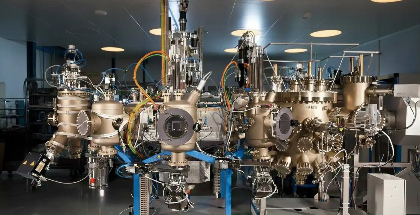
A typical MBE system consists of an ultra-high vacuum chamber, material sources, a substrate heating unit, shutters, and equipment for monitoring the growth process.
First, the crystalline substrate is cleaned to remove contaminants and surface oxide layers. It is then placed inside the vacuum chamber and heated to a temperature suitable for the material being fabricated.
Material sources such as Gallium (Ga), Aluminum (Al), Indium (In), and Arsenic (As) are heated separately in specialized containers known as Effusion Cells. Once they reach the appropriate temperatures, they generate atomic or molecular beams directed toward the substrate.
At the substrate surface, atoms attach and arrange themselves according to the existing crystal lattice. This process continues until the desired layer thickness is achieved.
One notable feature of an MBE system is its use of mechanical shutters to open or close the paths of individual material beams. This allows operators to change the composition of semiconductor layers within a very short time, making it possible to create structures consisting of multiple layers of different materials.
To monitor this process, some systems use RHEED (Reflection High-Energy Electron Diffraction). This technique directs a high-energy electron beam onto the sample surface and analyzes the resulting diffraction pattern, providing information about the surface condition and crystal growth process.
The ability to control individual material sources and monitor the growth process is what enables MBE to produce highly precise semiconductor structures.
3. What Are the Main Applications of MBE Technology ?
One of the most important applications of MBE is the fabrication of semiconductor heterostructures. These structures consist of multiple layers of different semiconductor materials stacked together. For example, combining GaAs and AlGaAs can create interfaces with different electronic properties.
By precisely controlling the thickness and composition of each layer, researchers can adjust how electrons and holes move through the material. This provides the foundation for developing semiconductor devices with specialized performance characteristics.
Applications in High-Speed Transistors
MBE is used to fabricate material structures for High Electron Mobility Transistors (HEMTs).
In these transistors, combining two different semiconductor layers can create a two-dimensional electron gas (2DEG). Electrons become concentrated and move within an extremely thin region at the interface between the materials. By reducing scattering during electron transport, this structure can achieve high electron mobility.
HEMT devices are widely used in telecommunications equipment, radar systems, signal amplifiers, and other high-frequency electronic applications.
Applications in Semiconductor Lasers and Optoelectronics
Another important application of MBE is the development of quantum well structures. In these structures, an extremely thin semiconductor layer is sandwiched between two layers of materials with wider bandgaps.
This arrangement changes the energy states of electrons and holes, allowing researchers to control the light emission and absorption characteristics of the material.
Quantum well structures are used in semiconductor lasers, photodetectors, and various optoelectronic devices for optical communications. Precise control over the thickness of each layer allows researchers to adjust the operating wavelength of a device according to specific requirements.
Research into Nanomaterials and Quantum Technologies
As semiconductor structures shrink to the nanometer scale, quantum effects become increasingly significant. MBE enables the fabrication of structures such as quantum wires, quantum dots, and semiconductor superlattices.
These structures are being investigated for applications in photonics, single-photon emission devices, and quantum computing hardware. The ability to control individual material layers makes MBE a suitable technique for experimenting with complex semiconductor architectures.
4. Advantages and Limitations of MBE Compared with Other Epitaxy Techniques
Compared with many thin-film growth techniques, MBE offers significant advantages in controlling material structures. Supplying atoms from separate sources allows engineers to precisely adjust the composition and thickness of each layer. The ultra-high vacuum environment also minimizes contamination, helping produce materials with high purity.
However, MBE is not suitable for every manufacturing process. Its growth rate is relatively slow, while the vacuum system and material sources require substantial investment. Operation also requires specialized personnel to control temperature, pressure, and other parameters throughout the fabrication process.
A comparison with MOCVD (Metal-Organic Chemical Vapor Deposition), another widely used epitaxy technology, highlights several important differences. MOCVD uses gaseous chemical precursors to form material layers on a substrate and generally offers higher growth rates and better scalability for large-scale production. In contrast, MBE has an advantage in controlling material composition and layer thickness at the atomic level.
As a result, MBE is often selected for new material research, the development of complex semiconductor structures, and the fabrication of specialized devices. MOCVD, meanwhile, is widely used in large-scale manufacturing processes, particularly for materials such as GaN and various LED structures.
5. What Role Does Measurement and Testing Play in MBE Material Research ?
After the MBE growth process is completed, the resulting material layers must undergo several testing procedures to determine their quality. A sample with a crystal structure that matches the design does not necessarily meet all the required electrical or optical performance specifications.
For example, in semiconductor heterostructures, researchers need to measure electron mobility and carrier concentration to evaluate electrical conductivity. For quantum well structures, light absorption and emission characteristics must be analyzed to determine how the material performs.
Techniques such as X-ray Diffraction (XRD), Transmission Electron Microscopy (TEM), Hall Effect measurements, and Photoluminescence (PL) spectroscopy are commonly used to analyze crystal structures, material composition, and the electrical and optical properties of semiconductor materials.
When moving to the device fabrication stage, electrical measurement instruments and signal analysis equipment are further used to evaluate current-voltage characteristics, frequency response, switching behavior, and operational stability.
For power semiconductor devices and high-frequency components, testing also helps identify operational abnormalities, evaluate performance limits, and determine the causes of efficiency degradation.
Therefore, semiconductor research does not end with producing a material layer that meets the design specifications. Measurement and testing results provide the basis for determining whether the resulting structure is truly suitable for its intended application.
6. From Material Research to Practical Semiconductor Device Testing at Tektronix Semiconductor 2026
MBE demonstrates how modern semiconductor technology requires precise material control at extremely small scales. However, when moving from materials to semiconductor devices and electronic systems, measurement requirements become increasingly complex.
This is particularly important for wide-bandgap semiconductor materials such as SiC and GaN, where engineers need to evaluate various parameters related to voltage, current, switching losses, signal response, and device reliability.
These topics are also among the key areas of interest at Tektronix Semiconductor 2026, a seminar jointly organized by EMIN and Tektronix. The program focuses on practical challenges in semiconductor research, development, and technology validation, ranging from innovations in transistor measurement and testing to failure analysis of SiC/GaN materials.
In addition to technical presentations, attendees will have the opportunity to explore and experience several measurement and testing instruments firsthand.
Through these demonstrations, engineers and researchers can gain further insights into instrument selection, measurement setup, and the evaluation of semiconductor device characteristics in practical research applications.
Tektronix Semiconductor 2026 Seminar Information
Date: November 11, 2026.
Venue: National Innovation Center (NIC), Hanoi, Vietnam.
Organizers: EMIN in collaboration with Tektronix.
Target Audience: Electronics engineers, semiconductor engineers, R&D specialists, lecturers, and researchers.
View the event agenda and registration details at here