The growth of electric vehicles, artificial intelligence, renewable energy, and power electronics is driving global demand for semiconductor devices. This trend is also creating numerous career opportunities for electrical and electronics engineers, particularly in semiconductor research, IC design, testing, and electronic system development.
However, conventional knowledge of electrical circuits and electronic systems alone is not sufficient to meet all the requirements of the semiconductor industry. Engineers need a deeper understanding of semiconductor physics, device operating principles, signal characteristics, and component-level testing and measurement techniques.
So, what additional knowledge and skills should electrical engineers acquire to enter this field?
1. Master Semiconductor Physics and Device Operating Principles
Semiconductor physics is the foundation for understanding how electronic components are formed and how they operate. Unlike conventional conductive or insulating materials, the electrical conductivity of semiconductors can be controlled through doping, temperature changes, and electric fields.
The two basic types of semiconductor materials are P-type and N-type semiconductors. When these two regions come into contact, a depletion region forms at the junction, creating an internal electric field. This is the fundamental operating principle of the P-N junction, which is used in diodes and many other semiconductor device structures.
For transistors, engineers need to understand how control voltage affects the current flowing through a device. For example, in a MOSFET, the voltage applied to the gate terminal changes the conductivity of the channel between the source and drain terminals. Parameters such as threshold voltage, leakage current, on-state resistance, and parasitic capacitance directly determine device performance.
In addition to conventional silicon, semiconductor materials such as silicon carbide (SiC) and gallium nitride (GaN) are becoming increasingly widespread. Thanks to their wide bandgap properties, these materials can meet demanding voltage, temperature, and high-speed switching requirements in appropriately designed applications.
Understanding the relationship between material structure and electrical characteristics enables engineers not only to use semiconductor devices effectively but also to investigate why a device may behave differently from its intended design.
2. Strengthen Knowledge of Electronics and IC Design
Electrical engineers already have a solid foundation in circuit theory. However, entering the semiconductor industry requires a shift from system-level analysis toward studying device characteristics and the functional blocks within integrated circuits.
For analog circuits, key parameters include gain, impedance, linearity, noise, and stability. In digital circuits, factors such as logic levels, signal propagation delay, setup time, and hold time are essential for ensuring accurate data processing.
As operating frequencies increase, the effects of parasitic capacitance, interconnect inductance, and signal reflections become more significant. A circuit trace that can be considered an ideal connection at low frequencies may cause signal distortion at higher switching speeds.
Therefore, engineers need to understand signal integrity, evaluate waveforms and amplitudes, and analyze rise times and noise during signal transmission.
For engineers with a background in power electronics, knowledge of DC-DC converters, inverters, and switching control is also a significant advantage. These fields rely heavily on power semiconductor devices and are directly related to SiC/GaN applications in electric vehicles, chargers, and energy systems.
3. Understand Semiconductor Manufacturing Processes and Factors Affecting Device Quality
The semiconductor manufacturing process typically involves wafer preparation, oxidation, photolithography, doping, thin-film deposition, etching, and the formation of metal interconnect layers.
Each stage can affect the quality of the final product. For example, deviations during photolithography can alter device dimensions, subsequently affecting parasitic resistance and capacitance. Similarly, inappropriate doping concentrations or depths can change threshold voltage, leakage current, and voltage-blocking capability.
After fabrication, the packaging process also has a significant impact on device reliability. For power semiconductor devices, thermal resistance, heat dissipation capability, and junction temperature are critical factors that determine operating limits.
Understanding these factors helps engineers distinguish between failures originating from device structures, manufacturing processes, packaging, or operating conditions.
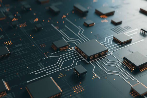
4. Explore SiC/GaN Semiconductor Technologies and Failure Analysis
SiC and GaN are driving significant changes in the field of power electronics. Thanks to their material properties, these devices can operate at high voltages, temperatures, and switching frequencies in many applications where conventional silicon devices face limitations.
SiC is commonly used in electric vehicle inverters, high-power converters, and industrial power systems. GaN offers advantages in many high-frequency switching applications, particularly power supplies that require compact designs and high power density.
However, high switching speeds also place greater demands on gate driver design, parasitic inductance control, and electromagnetic interference (EMI) management. Phenomena such as voltage ringing, transient currents, and voltage stress can affect device reliability.
Therefore, engineers need the ability to measure dynamic characteristics, determine switching losses, and evaluate device performance under different load and temperature conditions.
In addition, failure analysis is an essential skill in the validation process. When a device exhibits abnormal leakage current or unstable operation, engineers must identify the possible causes, which may originate from the material, device structure, manufacturing process, thermal conditions, or even the measurement system itself.
5. Master Semiconductor Measurement and Testing Techniques
To work in the semiconductor industry, electrical engineers need to combine knowledge of device physics, electronics, measurement techniques, and experimental data analysis. Among these areas, testing and measurement play a vital role throughout the entire process, from material research and device development to IC validation and product reliability assessment.
One fundamental measurement technique is the current-voltage (I-V) characterization. By varying the voltage applied to a device and recording the corresponding current, engineers can determine threshold voltage, leakage current, on-state resistance, and potential abnormalities.
Meanwhile, an oscilloscope allows engineers to observe signals over time and analyze switching behavior, overshoot, noise, and oscillations in a circuit. When measuring signals with fast switching edges, the instrument's bandwidth and sampling rate must be sufficiently high to minimize waveform measurement errors. Probes must also be selected carefully, as their input capacitance can affect the signal being measured.
A Source Measure Unit (SMU) can both supply power and measure voltage or current. It is commonly used to characterize semiconductor devices under various bias conditions.
We invite engineers and semiconductor professionals to attend the Tektronix Semiconductor 2026 Seminar in Hanoi.
The seminar will focus on semiconductor testing and measurement technologies, covering topics ranging from transistor development to artificial intelligence systems, as well as wide-bandgap semiconductor materials such as SiC/GaN and failure analysis methods from the material level to individual devices.
The event will also feature live equipment demonstrations and technical discussions with Tektronix experts. Participants will have the opportunity to explore measurement methods, learn how to select appropriate test equipment, and gain insights into the technical requirements for semiconductor device and system validation.
Seminar Information:
Time: 09:00 – 14:00, November 11, 2026
Venue: 6th Floor, NIC Building, Alley 7 Ton That Thuyet Street, Cau Giay District, Hanoi, Vietnam
Organizers: EMIN in collaboration with Tektronix
Admission: Free of charge
Registration: https://emin.vn/hoi-thao-tektronix-semiconductor-2026-2286/ne.html