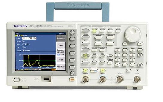
Tektronix AFG3021C 任意函数发生器(25 MHz,1CH,250MS / s)
制造商: TEKTRONIX Model: AFG3021C - 联系
Channels: 1
Waveforms: Sine, Square, Pulse, Ramp, Triangle, Sin(x)/x, Exponential Rise and Decay, Gaussian, Lorentz, Haversine, DC, Noise
Sample Rate: 2 to 128K:250MS/s
Sine Wave: 1 µHz to 25 MHz
Square Wave: 1 µHz to 25 MHz
Ramp Wave: 1 µHz to 500 kHz
Pulse Wave: 1 mHz to 25 MHz
Other Waveforms: 1 µHz to 500 kHz
Arbitrary Waveforms: 1 mHz to 12.5 MHz
Amplitude Range (50Ω load): 10 mVp-p to 10 Vp-p
Range (open circuit or High Z): 20 mVp-p to 20 Vp-p
Modulation: AM, FM, PM, FSK, PWM
Display: 5.6 in. Color TFT LCD
Power Source: 100-240 V, 47-63 Hz
Power Consumption: Less than 120 W
Dimensions: 156.3 x 329.6 x 168.0 mm
Weight: 4.5 kg
Includes: Quick-start user manual, power cord, USB cable, CD-ROM with specifications and performance verification manual, programmer manual, service manual, LabView and IVI drivers, CD-ROM with ArbExpress™ software, and NIST-traceable calibration certificate. Please specify power plug when ordering.
Option:
Rackmount Kit: RM3100
Fuse adapter, BNC-P to BNC-R: 013-0345-xx
Fuse set, 3 pcs, 0.125 A: 159-0454-xx
BNC cable shielded, 3 ft: 012-0482-xx
BNC cable shielded, 9 ft: 012-1256-xx
GPIB cable, double shielded: 012-0991-xx
50 O BNC terminator: 011-0049-02
Characteristics
AFG3000C Series Characteristics
|
Characteristic |
AFG3011C |
AFG3021C AFG3022C |
AFG3051C AFG3052C |
AFG3101C AFG3102C |
AFG3251C AFG3252C |
|---|---|---|---|---|---|
|
Channels |
1 |
1 / 2 |
1 / 2 |
1 / 2 |
1 / 2 |
|
Waveforms |
Sine, Square, Pulse, Ramp, Triangle, Sin(x)/x, Exponential Rise and Decay, Gaussian, Lorentz, Haversine, DC, Noise |
||||
|
Sine Wave |
1 µHz to 10 MHz |
1 µHz to 25 MHz |
1 µHz to 50 MHz |
1 µHz to 100 MHz |
1 µHz to 240 MHz |
|
Sine wave in Burst Mode |
1 µHz to 5 MHz |
1 µHz to 12.5 MHz |
1 µHz to 25 MHz |
1 µHz to 50 MHz |
1 µHz to 120 MHz |
|
Effective maximum frequency out |
10 MHz |
25 MHz |
50 MHz |
100 MHz |
240 MHz |
|
Amplitude Flatness (1 Vp-p) |
<5 mhz:="" 0="" 15="" db="" p=""> ≥5 MHz to 10 MHz: ±0.3 dB |
<5 mhz:="" 0="" 15="" db="" p=""> ≥5 MHz to 20 MHz: ±0.3 dB ≥20 MHz to 25 MHz: ±0.5 dB |
<5 mhz:="" 0="" 15="" db="" p=""> ≥5 MHz to 45 MHz: ±0.3 dB ≥45 MHz to 50 MHz: ±0.5 dB |
<5 mhz:="" 0="" 15="" db="" p=""> ≥5 MHz to 25 MHz: ±0.3 dB ≥25 MHz to 100 MHz: ±0.5 dB |
<5 mhz:="" 0="" 15="" db="" p=""> ≥5 MHz to 25 MHz: ±0.3 dB ≥25 MHz to 100 MHz: ±0.5 dB ≥100 MHz to 200 MHz: ±1.0 dB ≥200 MHz to 240 MHz: ±2.0 dB |
|
Harmonic Distortion (1 Vp-p)
|
10 Hz to 20 kHz: < -60 dBc ≥20 kHz to 1 MHz: < -55 dBc ≥1 MHz to 5 MHz: < -45 dBc ≥5 MHz to 10 MHz: < -45 dBc |
10 Hz to 20 kHz: < -70 dBc ≥20 kHz to 1 MHz: < -60 dBc ≥1 MHz to 10 MHz: < -50 dBc ≥10 MHz to 25 MHz: < -40 dBc |
10 Hz to 20 kHz: < -70 dBc ≥20 kHz to 1 MHz: < -60 dBc ≥1 MHz to 5 MHz: < -50 dBc ≥5 MHz to 50 MHz: < -40 dBc |
10 Hz to 1 MHz: < -60 dBc ≥1 MHz to 5 MHz: < -50 dBc ≥5 MHz to 100 MHz: < -37 dBc |
10 Hz to 1 MHz: < -60 dBc ≥1 MHz to 5 MHz: < -50 dBc ≥5 MHz to 25 MHz: < -37 dBc ≥25 MHz to 240 MHz: < -30 dBc |
|
THD |
<0.2% (10 Hz – 20 kHz, 1 Vp-p) |
||||
|
Spurious (1 Vp-p) |
10 Hz to 1 MHz: < -60 dBc ≥1 MHz to 10 MHz: < -50 dBc |
10 Hz to 1 MHz: < -60 dBc ≥1 MHz to 25 MHz: < -50 dBc |
10 Hz to 1 MHz: < -60 dBc ≥1 MHz to 50 MHz: < -50 dBc |
10 Hz to 1 MHz: < -60 dBc ≥1 MHz to 25 MHz: < -50 dBc ≥25 MHz to 100 MHz: < - 50 dBc + 6 dBc/octave |
10 Hz to 1 MHz: < -50 dBc ≥1 MHz to 25 MHz: < -47 dBc ≥25 MHz to 240 MHz: < - 47 dBc + 6 dBc/octave |
|
Phase noise, typical |
< -110 dBc/Hz at 10 MHz, 10 kHz offset, 1 Vp-p |
< -110 dBc/Hz at 20 MHz, 10 kHz offset, 1 Vp-p |
|||
|
Residual clock noise |
-63 dBm |
-63 dBm |
-63 dBm |
-57 dBm |
-57 dBm |
|
Square Wave |
1 µHz to 5 MHz |
1 µHz to 25 MHz |
1 μHz to 40 MHz |
1 µHz to 50 MHz |
1 µHz to 120 MHz |
|
Rise/Fall time |
≤50 ns |
≤9 ns |
≤7 ns |
≤5 ns |
≤2.5 ns |
|
Jitter (RMS), typical |
500 ps |
500 ps |
300 ps |
200 ps |
100 ps |
|
Ramp Wave |
1 µHz to 100 kHz |
1 µHz to 500 kHz |
1 μHz to 800 kHz |
1 µHz to 1 MHz |
1 µHz to 2.4 MHz |
|
Linearity, typical |
≤0.2% of peak output |
≤0.1% of peak output |
≤ 0.1% of peak output |
≤0.15% of peak output |
≤0.2% of peak output |
|
Symmetry |
0.0% to 100.0% |
||||
|
Pulse Wave |
1 mHz to 5 MHz |
1 mHz to 25 MHz |
1 mHz to 40 MHz |
1 mHz to 50 MHz |
1 mHz to 120 MHz |
|
Pulse width |
80.00 ns to 999.99 s |
16.00 ns to 999.99 s |
12 ns to 999.99 s |
8.00 ns to 999.99 s |
4.00 ns to 999.99 s |
|
Resolution |
10 ps or 5 digits |
||||
|
Pulse duty |
0.001% to 99.999% (Limitations of pulse width apply) |
||||
|
Edge transition time |
50 ns to 625 s |
9 ns to 625 s |
7 ns to 625 s |
5 ns to 625 s |
2.5 ns to 625 s |
|
Resolution |
10 ps or 4 digits |
||||
|
Lead delay |
|
||||
|
Range |
(Continuous Mode): 0 ps to Period (Triggered/Gated Burst Mode): 0 ps to Period – [Pulse Width + 0.8 * (Leading Edge Time + Trailing Edge Time)] |
||||
|
Resolution |
10 ps or 8 digits |
||||
|
Overshoot, typical |
<5% |
||||
|
Jitter (RMS), typical |
500 ps |
500 ps |
300 ps |
200 ps |
100 ps |
|
Other Waveforms |
1 µHz to 100 kHz |
1 µHz to 500 kHz |
1 μHz to 800 kHz |
1 µHz to 1 MHz |
1 µHz to 2.4 MHz |
|
Noise Bandwidth (-3 dB) |
10 MHz |
25 MHz |
50 MHz |
100 MHz |
240 MHz |
|
Noise type |
White Gaussian |
||||
|
Internal Noise Add |
When activated, output signal amplitude is reduced to 50% |
||||
|
Level |
0.0% to 50% of amplitude (Vp-p) setting |
||||
|
Resolution |
1% |
||||
|
DC (into 50 Ω) |
-10 V to +10 V |
-5 V to +5 V |
–5 V to +5 V |
-5 V to +5 V |
-2.5 V to +2.5 V |
|
Arbitrary Waveforms |
1 mHz to 5 MHz |
1 mHz to 12.5 MHz |
1 mHz to 25 MHz |
1 mHz to 50 MHz |
1 mHz to 120 MHz |
|
Arbitrary waveforms in Burst Mode |
1 mHz to 2.5 MHz |
1 mHz to 6.25 MHz |
1 mHz to 12.5 MHz |
1 mHz to 25 MHz |
1 mHz to 60 MHz |
|
Effective analog bandwidth (-3 dB) |
8 MHz |
70 MHz |
100 MHz |
225 MHz |
|
|
Nonvolatile memory |
4 waveforms |
||||
|
Memory: Sample rate (1K=1024 points) |
2 to 128 K: 250 MS/s |
2 to 128 K: 250 MS/s |
2 to 16 K: 1 GS/s >16 K to 128 K: 250 MS/s |
2 to 16 K: 1 GS/s >16 K to 128 K: 250 MS/s |
2 to 16 K: 2 GS/s >16 K to 128 K: 250 MS/s |
|
Vertical resolution |
14 bits |
||||
|
Rise/Fall time |
≤80 ns |
≤14 ns |
≤10 ns |
≤8 ns |
≤3 ns |
|
Jitter (RMS), typical |
4 ns |
4 ns |
1 ns at 1 GS/s 4 ns at 250 MS/s |
1 ns at 1 GS/s 4 ns at 250 MS/s |
500 ps at 2 GS/s 4 ns at 250 MS/s |
|
Amplitude |
|||||
|
Range (50 Ω load) |
20 mVp-p to 20 Vp-p |
10 mVp-p to 10 Vp-p |
10 mVp-p to 10 Vp-p |
20 mVp-p to 10 Vp-p |
≤200 MHz: 50 mVp-p to 5 Vp-p >200 MHz: 50 mVp-p to 4 Vp-p |
|
Range (open circuit or High Z) |
40 mVp-p to 40 Vp-p |
20 mVp-p to 20 Vp-p |
20 mVp-p to 20 Vp-p |
40 mVp-p to 20 Vp-p |
≤200 MHz: 100 mVp-p to 10 Vp-p >200 MHz: 100 mVp-p to 8 Vp-p |
|
Accuracy |
±(2% of setting +2 mV) (1 kHz sine wave, 0 V offset, >20 mVp-p amplitude) |
±(1% of setting +1 mV) (1 kHz sine wave, 0 V offset, >10 mVp-p amplitude) |
|||
|
Resolution |
0.1 mVp-p, 0.1 mVRMS, 1 mV, 0.1 dBm or 4 digits |
||||
|
Units |
Vp-p, VRMS, dBm (sine wave only) and Volt (high/low setting) |
||||
|
Output impedance |
50 Ω |
||||
|
Load impedance setting |
Selectable: 50 Ω, 1Ω to 10.0 kΩ, High Z (Adjusts displayed amplitude according to selected load impedance) |
||||
|
Isolation |
<42 v="" sub="">pk maximum to earth |
||||
|
Short-circuit protection |
Signal outputs are robust against permanent shorts against floating ground |
||||
|
External voltage protection |
To protect signal outputs against external voltages use fuse adapter 013-0345-xx |
||||
|
DC Offset |
|||||
|
Range (50 Ω load) |
±(10 Vpk – Amplitudepp/2) |
±(5 Vpk – Amplitudepp/2) |
±(5 Vpk – Amplitudepp/2) |
±5 Vpk DC |
±2.5 Vpk DC |
|
Range (open circuit or High Z) |
±(20 Vpk – Amplitudepp/2) |
±(10 Vpk – Amplitudepp/2) |
±(10 Vpk – Amplitudepp/2) |
±10 Vpk DC |
±5 Vpk DC |
|
Accuracy |
±(2% of |setting| + 10 mV + 1% of amplitude (Vp-p)) |
±(1% of |setting| + 5 mV + 0.5% of amplitude (Vp-p)) |
|||
|
Resolution |
1 mV |
||||
System Characteristics
|
Characteristic |
Description |
||
|---|---|---|---|
|
Frequency Resolution |
1 μHz or 12 digits |
||
|
Internal Frequency Reference |
|||
|
Stability |
All except ARB: ±1 ppm, 0 °C to 50 °C ARB: ±1 ppm ± 1 µHz, 0 °C to 50 °C |
||
|
Aging |
±1 ppm per year |
||
|
Phase (except DC, Noise, Pulse) |
|||
|
Range |
-180° to +180° |
||
|
Resolution |
0.01° (sine), 0.1° (other waveforms) |
||
|
|
When activated, output signal amplitude is reduced to 50% |
||
|
Level |
0.0% to 50% of amplitude (Vp-p) setting |
||
|
Resolution |
1% |
||
|
Main Output |
50 Ω |
||
|
Remote Programming |
GPIB, LAN 10BASE-T / 100BASE-TX, USB 1.1 Compatible with SCPI-1999.0 and IEEE 488-2 standards |
||
|
Configuration times, max typical |
USB |
LAN |
GPIB |
|
Function change |
81 ms |
81 ms |
81 ms |
|
Frequency change (except Pulse) |
2.5 ms |
6 ms |
3.2 ms |
|
Frequency change (Pulse) |
40 ms |
37 ms |
32 ms |
|
Amplitude change |
90 ms |
97 ms |
90 ms |
|
Select user ARB (4k points from USB Memory) |
48 ms |
50 ms |
49 ms |
|
Select user ARB (128k points from USB Memory) |
260 ms |
266 ms |
240 ms |
|
Data download time for 4000 point waveform data, typical |
47 ms |
78 ms |
320 ms |
|
Power Source |
100-240 V, 47-63 Hz, or 115 V, 360-440 Hz |
||
|
Power Consumption |
Less than 120 W |
||
|
Warm-up Time, typical |
20 minutes |
||
|
Power-on Self Diagnostics, typical |
<10 s="" p=""> |
||
|
Acoustic Noise, typical |
<50 dba="" p=""> |
||
|
Display |
5.6 in. Color TFT LCD |
||
|
User Interface and Help Languages |
English, French, German, Japanese, Korean, Portuguese, Simplified and Traditional Chinese, Russian (user selectable) |
||
Modulation
Modulation: Max FM Peak Deviation
|
Characteristic |
AFG3011C |
AFG3021C AFG3022C |
AFG3051C AFG3052C |
AFG3101C AFG3102C |
AFG3251C AFG3252C |
|---|---|---|---|---|---|
|
Sine |
5 MHz |
12.5 MHz |
25 MHz |
50 MHz |
120 MHz |
|
Square |
2.5 MHz |
12.5 MHz |
20 MHz |
25 MHz |
60 MHz |
|
ARB |
2.5 MHz |
6.25 MHz |
12.5 MHz |
25 MHz |
60 MHz |
|
Others |
50 kHz |
250 kHz |
400 kHz |
500 kHz |
1.2 MHz |
AM, FM, PM
|
Characteristic |
Description |
|---|---|
|
Carrier Waveforms |
All, except Pulse, Noise, and DC |
|
Source |
Internal/External |
|
Internal Modulating Waveform |
Sine, square, ramp, noise, ARB (AM: maximum waveform length 4,096; FM/PM: maximum waveform length 2,048) |
|
Internal Modulating Frequency |
2 mHz to 50.00 kHz |
|
AM Modulation Depth |
0.0% to +120.0% |
|
Min FM Peak Deviation |
DC |
|
Max FM Peak Deviation |
See following table, Modulation: Max FM Peak Deviation |
|
PM Phase Deviation |
-360.0° to +360.0° |
Pulse Width Modulation
|
Characteristic |
Description |
|---|---|
|
Carrier Waveform |
Pulse |
|
Source |
Internal/External |
|
Internal Modulating Waveform |
Sine, square, ramp, noise, ARB (maximum waveform length 2,048) |
|
Internal Modulating Frequency |
2 mHz to 50.00 kHz |
|
Deviation |
0% to 50.0% of pulse period |
Sweep: Max Start/Stop Frequency
|
Characteristic |
AFG3011C |
AFG3021C AFG3022C |
AFG3051C AFG3052C |
AFG3101C AFG3102C |
AFG3251C AFG3252C |
|---|---|---|---|---|---|
|
Sine |
10 MHz |
25 MHz |
50 MHz |
100 MHz |
240 MHz |
|
Square |
5 MHz |
25 MHz |
40 MHz |
50 MHz |
120 MHz |
|
ARB |
5 MHz |
12.5 MHz |
25 MHz |
50 MHz |
120 MHz |
|
Others |
100 kHz |
500 kHz |
800 kHz |
1 MHz |
2.4 MHz |
Frequency Shift Keying
|
Characteristic |
Description |
|---|---|
|
Carrier Waveforms |
All, except Pulse, Noise, and DC |
|
Source |
Internal/External |
|
Internal Modulating Frequency |
2 mHz to 1.000 MHz |
|
Number of Keys |
2 |
Sweep
|
Characteristic |
Description |
|---|---|
|
Waveforms |
All, except Pulse, Noise, and DC |
|
Type |
Linear, logarithmic |
|
Sweep Time |
1 ms to 300 s |
|
Hold/Return Time |
0 ms to 300 s |
|
Max Total Sweep Time |
300 s |
|
Resolution |
1 ms or 4 digits |
|
Total Sweep Time Accuracy, typical |
≤0.4% |
|
Min Start/Stop Frequency |
All except ARB: 1 µHz ARB: 1 mHz |
|
Max Start/Stop Frequency |
See chart, below |
Burst
|
Characteristic |
Description |
|---|---|
|
Waveforms |
All, except Noise and DC |
|
Type |
Triggered, gated (1 to 1,000,000 cycles or Infinite) |
|
Internal Trigger Rate |
1 μs to 500.0 s |
|
Gate and Trigger Sources |
Internal, external, remote interface |
Auxiliary Inputs
|
Characteristic |
Description |
|---|---|
|
Modulation Inputs Channel 1, Channel 2 |
|
|
Input range |
All except FSK: ±1 V FSK: 3.3 V logic level |
|
Impedance |
10 kΩ |
|
Frequency range |
DC to 25 kHz (122 kS/s) |
|
External Triggered/Gated Burst Input |
|
|
Level |
TTL compatible |
|
Impedance |
10 kΩ |
|
Pulse width |
100 ns minimum |
|
Slope |
Positive/Negative, selectable |
|
Trigger delay |
0.0 ns to 85.000 s |
|
Resolution |
100 ps or 5 digits |
|
Jitter (RMS), typical |
Burst: <500 ps="" trigger="" input="" to="" signal="" output="" p=""> |
|
10 MHz Reference Input |
|
|
Impedance |
1 kΩ, AC coupled |
|
Required Input Voltage Swing |
100 mVp-p to 5 Vp-p |
|
Lock Range |
10 MHz ±35 kHz |
|
External Add Input (CH1) |
AFG3101C, AFG3102C, AFG3251C, AFG3252C only |
|
Impedance |
50 Ω |
|
Input range |
-1 V to +1 V (DC + peak AC) |
|
Bandwidth |
DC to 10 MHz (-3 dB) at 1 Vp-p |
Auxiliary Outputs
|
Characteristic |
Description |
|---|---|
|
Trigger Output (Channel 1) |
|
|
Level |
Positive TTL level pulse into 1 kΩ |
|
Impedance |
50 Ω |
|
Jitter (RMS), typical |
AFG3011C/21C/22C: 500 ps AFG3051C/52C: 300ps AFG3101C/02C: 200 ps AFG3251C/52C: 100 ps |
|
Max Frequency |
4.9 MHz (4.9 MHz to 50 MHz: A fraction of the frequency is output; >50 MHz: no signal is output) |
|
Clock Reference Out (10 MHz) |
AFG3101C, AFG3102C, AFG3251C, AFG3252C only |
|
Impedance |
50 Ω, AC coupled |
|
Amplitude |
1.2 Vp-p into 50 Ω load |
Physical Characteristics
Benchtop Configuration
|
Dimensions |
mm |
in. |
|---|---|---|
|
Height |
156.3 |
6.2 |
|
Width |
329.6 |
13.0 |
|
Depth |
168.0 |
6.6 |
|
Weight |
kg |
lb. |
|
Net |
4.5 |
9.9 |
|
Shipping |
5.9 |
12.9 |
Environmental and Safety Characteristics
|
Characteristic |
Description |
|---|---|
|
Temperature |
|
|
Operating |
0 °C to +50 °C |
|
Nonoperating |
-30 °C to +70 °C |
|
Humidity |
|
|
Operating |
≤ +40 °C: ≤80% > +40 °C to 50 °C: ≤60% |
|
Altitude |
Up to 10,000 ft./3,000 m |
|
EMC Compliance |
|
|
European Union |
EU Council Directive 2004/108/EC |
|
Safety |
UL 61010-1:2004 CAN/CSA C22.2 No. 61010-1:2004 IEC 61010-1:2001 |
- 质量承诺
- 正品保修
- 送货到家
- 交易简单化