Semiconductor Defect Inspection
Yield loss in wafer processing often starts with defects that are too small, too scattered, or too inconsistent to catch through manual review alone. In semiconductor manufacturing and incoming material control, inspection systems help teams detect scratches, particles, discoloration, process-related anomalies, and substrate defects earlier, with more repeatable documentation and clearer traceability.
Semiconductor Defect Inspection covers equipment used to identify and analyze defects on wafers and related substrates during different stages of production, qualification, and failure analysis. Depending on the task, this may involve fast surface screening, higher-resolution imaging, defect mapping, or non-destructive inspection methods for advanced materials.
Where defect inspection fits in semiconductor workflows
Defect inspection is relevant across IQC, process monitoring, outgoing quality checks, and engineering analysis. The goal is not only to find visible issues, but also to create consistent records of defect location, image data, and wafer condition so process teams can trace patterns back to equipment, handling, material quality, or process steps.
On a category level, these systems often overlap with Automated Optical Inspection (AOI) when high-throughput image-based screening is required. For more specialized needs, buyers may also compare solutions within broader defect inspection equipment workflows depending on wafer type, defect class, and required resolution.
Typical inspection tasks in this category
Inspection requirements vary by wafer material, defect size, and the production stage. Some applications focus on general surface screening for particles and scratches, while others require more advanced review of process defects, probe marks, bump geometry, or crystal-related defects in compound semiconductor substrates.
In practice, buyers often evaluate systems based on several factors: wafer size compatibility, handling method, imaging approach, defect sensitivity, data output, and whether the system is intended for in-line screening or deeper engineering analysis. Surface defect detection and defect record traceability are common priorities because both directly affect yield investigation and process control.
Representative SPIROX systems for defect inspection
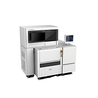
This category includes solutions from SPIROX, a manufacturer represented here with systems for wafer surface inspection, substrate defect analysis, and confocal-based measurement work. Rather than serving one single inspection method, the range illustrates how semiconductor defect inspection can span macro review, micro inspection, and material-specific analysis.
For example, the SPIROX MA6500 Macro Inspection System is geared toward rapid wafer surface review for issues such as particles, scratches, contamination, and discoloration on 8-inch and 12-inch wafers. The SPIROX MA6503D Micro Inspection System extends this concept with finer defect imaging and 3D-related inspection capability, supporting tasks such as bump height and coplanarity assessment alongside surface defect review.
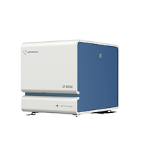
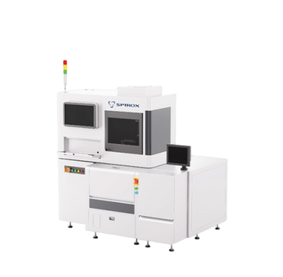
For SiC applications, the SPIROX SP3055A is positioned toward non-destructive inspection of crystal killer defects on SiC substrate or EPI wafers. In R&D or advanced analysis environments, the SPIROX SP8000A laser scanning confocal platform supports high-resolution measurement and optical analysis, which can be relevant when defect morphology or localized surface features need more detailed characterization.
How to choose the right inspection approach
The right system depends first on the inspection target. A production team screening standard silicon wafers for visible surface issues may prioritize speed, automation, wafer handling compatibility, and image archiving. An engineering group investigating recurring micro-defects may instead need higher imaging precision, coordinate accuracy, and better review tools for root-cause analysis.
Material type also matters. SiC and other advanced substrates can introduce defect modes that differ from conventional wafer surface contamination or scratch inspection. In these cases, the selection process should consider whether the equipment is intended for general optical inspection or for more specialized defect classes such as crystal-originated defects, structural anomalies, or topography-related issues.
It is also useful to think in terms of workflow integration. Some buyers need a station mainly for incoming material checks, while others need equipment that supports process development, defect database creation, or correlation with broader thermal test workflows and reliability evaluation. Matching the system to the actual inspection objective usually matters more than simply choosing the highest available resolution.
Key features that matter in B2B evaluation
When comparing semiconductor defect inspection equipment, several practical points usually drive the decision. Wafer compatibility is one of the first checks, including supported diameters, thickness ranges, and cassette or FOUP handling requirements. This is especially important for facilities that handle multiple wafer formats or need automated loading support.
Another major factor is inspection output. Many teams need more than a pass/fail result; they need defect images, coordinate records, OCR-related wafer identification, and review data that can be shared across quality, engineering, and process teams. Systems that support structured image output and clear defect documentation can make follow-up analysis more efficient.
Finally, consider whether the application calls for 2D image inspection, 3D-related measurement, or confocal-style analysis. Each serves a different purpose. A faster macro-level system may be ideal for broad screening, while a micro-inspection or confocal platform is more suitable when the defect signature itself must be examined in greater detail.
Related equipment in the inspection ecosystem
Defect inspection rarely stands alone in a semiconductor environment. It often works alongside image-based screening, environmental control, and downstream analysis tools. For users planning a broader inspection setup, adjacent categories such as chiller systems may also be relevant where thermal stability supports equipment performance or process consistency.
In many facilities, category selection is part of building an inspection ecosystem rather than purchasing a single instrument in isolation. That is why it helps to compare not only optical performance, but also data flow, review capability, wafer handling, and the role each system will play within inspection, engineering, or quality assurance operations.
Who typically buys semiconductor defect inspection systems?
These systems are commonly evaluated by semiconductor fabs, OSATs, wafer manufacturers, materials labs, R&D centers, and quality departments responsible for incoming inspection or process verification. The exact need may differ, but the common requirement is reliable detection and documentation of defects that can affect yield, downstream processing, or final device performance.
For procurement and engineering teams, the most effective buying process usually starts with a clear definition of wafer type, expected defect class, throughput target, and review depth. That makes it easier to shortlist whether a macro inspection platform, a micro defect inspection system, or a more specialized non-destructive analysis tool is the better fit.
Conclusion
Choosing semiconductor defect inspection equipment is ultimately about aligning inspection capability with the real manufacturing or analysis task. Some applications require fast wafer-level screening, while others need detailed imaging, defect mapping, or specialized material inspection for advanced substrates such as SiC.
This category brings together solutions that support those different needs, from surface inspection to deeper analytical workflows. If you are comparing systems for wafer quality control, process monitoring, or engineering review, focusing on defect type, wafer handling, data output, and required inspection depth will lead to a more practical shortlist.
Get exclusive volume discounts, bulk pricing updates, and new product alerts delivered directly to your inbox.
By subscribing, you agree to our Terms of Service and Privacy Policy.
Direct access to our certified experts