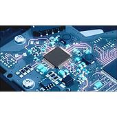
Background and practical needs
Recently, the topic of chip design in Vietnam has received much attention, especially after Prime Minister Pham Minh Chinh launched a program to encourage Vietnam to proactively design, manufacture and test necessary chip lines from now until 2027. This national strategic orientation is also an opportunity for universities, research centers and high-tech industries to invest heavily in human resources, infrastructure and chip manufacturing processes.
(Source: Government Newspaper)
One of the key factors is to train a generation of young engineers who are capable of accessing and operating the entire process chain from idea to finished chip product. In reality, in many units, the current infrastructure is still lacking and fragmented. If you want to turn a design idea into a viable product, you need a closed, synchronous process from design, simulation, manufacturing, measurement to performance evaluation and EMC testing.
EMIN is ready to provide a comprehensive set of solutions, including software, hardware, measurement equipment and technical support services, helping units fully implement chip making steps right in Vietnam.
Chip design with Cadence and Siemens software
The initial stage of the process is to design the chip in Vietnam on a specialized software platform. Cadence and Siemens are the world's leading toolkits, trusted by semiconductor companies, universities and R&D centers. This is the basis for projects from training scale to in-depth research.
At this stage, students or engineers can access both analog and digital design, expanding to specialized chip lines such as RFIC and MMIC for security and defense research, operating in very high frequency ranges from 20 GHz to 110 GHz, or even more.
The design process on Cadence includes defining electrical, thermal, RF and EMC requirements, preparing a PDK suitable for the manufacturing node such as 180nm or 65nm. The schematic is drawn using Virtuoso Schematic Editor, then simulating the electrical operation in DC, AC, Transient, Noise modes using Spectre simulator. Once the schematic is complete, the engineer proceeds to design the layout, following DRC and LVS checks to ensure accuracy. Parasitics are extracted using Cadence QRC or Assura to calculate the parasitic effects on the circuit before sending it to fabrication.
Electromagnetic field simulation and system optimization with ANSYS
Once the layout is complete, it is necessary to evaluate the impact of electromagnetic fields and parasitic effects on the entire system. This is a key step in the Cadence/ANSYS solution, helping to predict the actual performance of the chip when integrated into the PCB or finished product.
From Cadence, engineers export the layout data or 3D model in GDSII, OASIS or S-parameter format to import into ANSYS tools. HFSS is used to analyze RF/EM, S-parameters, radiation and electromagnetic compatibility. SIwave analyzes the integrity of high-speed signals and power supplies. Q3D Extractor calculates and reduces parasitic capacitance and inductance parameters. Icepak simulates and optimizes heat dissipation.
These results are fed back to Cadence for post-layout simulation, allowing for layout or schematic adjustments if needed, before the tape-out is sent to the foundry. Compliance with international standards such as MIL-STD or IEC 61967 at this stage helps ensure a highly reliable product.
Direct chip testing on wafer with probe station
When the chip is manufactured and returned in bare die or on wafer, chip testing with probe station is an indispensable step to verify parameters and performance.
Wafer testing system usually includes probe station with X-Y-Z moving table and vacuum system, microscope for precise observation and alignment, GSG, GS or coaxial microprobe suitable for the measurement frequency range. The measuring system comes with vector network analyzer (VNA), spectrum analyzer, signal generator from brands distributed by EMIN such as Rohde & Schwarz, Anritsu..., ensuring to meet the required frequency range.
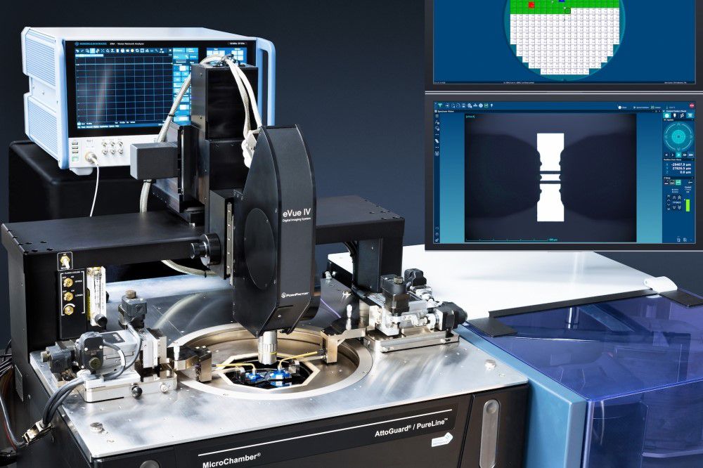
RF cable and standard adapter SMA, K, 2.4 mm or 1.85 mm ensure accurate signal transmission. The calibration kit corresponds to the probe type, with calibration substrate with standard pads Open, Short, Load, Thru, helping to calibrate SOLT, TRL or LRRM right at the probe tip.
The measurement procedure includes turning on the device, starting the system, mounting and connecting the probe, calibrating, placing the chip sample on the chuck (a thermal chuck is optional), aligning the measurement pad, lowering the probe contact enough to avoid scratching the pad, then scanning the frequency, adjusting the bias voltage or temperature as required. The measurement data is saved and analyzed by R&S, Keysight ADS or MATLAB for comparison with the simulation results.
Chip evaluation on PCB
Once the chip has been approved on the wafer, the next step is to mount the chip on the PCB for testing in a real integration environment. At this point, the Cadence - ANSYS solution continues to be used to simulate the electromagnetic operation of the chip when combined with other components, evaluate the impact of the PCB layout on signals and power, heat dissipation, as well as radiation phenomena. This result helps engineers refine the design before mass production.
EMC testing for chips and systems
For projects at key universities, chips and systems will be tested for EMC to assess electromagnetic compatibility. The EMC department performs measurements according to IEC, CISPR or MIL-STD standards, including conducted emission, radiated emission and immunity measurements.
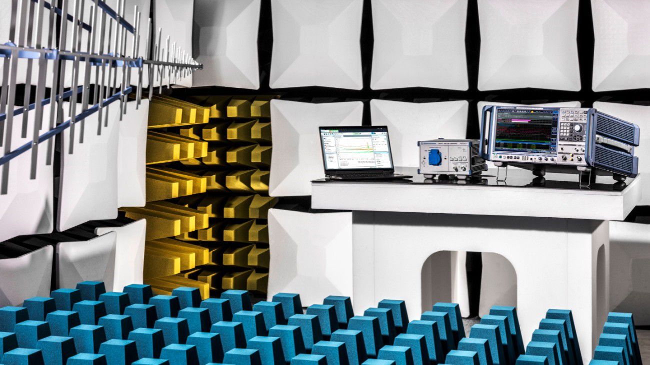
The EMC measurement results will be compared with simulations from Cadence/ANSYS solutions, helping to detect and correct deviations before releasing products to the market.
Complete solution from EMIN
EMIN provides full software, hardware and technical support for the entire process, from chip design in Vietnam, simulation with Cadence/ANSYS solutions, to chip testing with probe stations and EMC testing.
Conclude
The chip manufacturing process requires the coordination of many specialized tools and equipment. Having a synchronized solution will help shorten development time, improve accuracy and the ability to commercialize products.