Power-rail impedance measurement can be performed near a voltage regulator when the key concern is low-frequency behavior, such as control-loop resonance. A 2-port probing approach uses four contact points to support low-noise impedance measurements while requiring only limited changes to the PCB.
In the VDD_3V3_S0 example, the rail is a 3.3 V single-phase current-mode buck regulator supplied from 12 V and delivering 20.7 A to its load. Its energized, or ON-state, impedance is the critical trace for validating the rail behavior.
Summary: Measure low-frequency impedance near the regulator when that is the measurement objective. Calibrate with OPEN, SHORT, and 1 Ω LOAD steps. Evaluate the energized rail against its impedance target and check for sharp parallel resonances. At higher frequencies, probe-tip consistency and port-isolation calibration become important.
Why can a power rail be measured near the voltage regulator instead of at the load?
Impedance at the load is ideally the most relevant location, but measurement near the voltage regulator can be appropriate when low-frequency impedance is the primary concern. For VDD_3V3_S0, this approach was used to examine behavior such as control-loop resonance and can require minimal PCB modification.
The PCB solder mask was removed to create a probing port on VDD_3V3_S0. This created direct access for the probe at the selected measurement location without describing a redesign of the board.
What calibration method was used for the low-frequency impedance measurement?
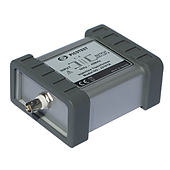
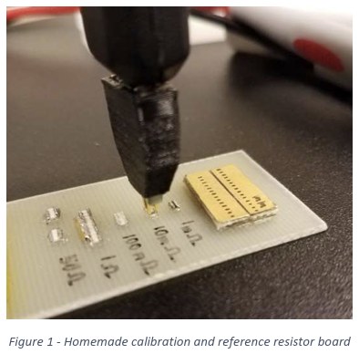
The setup used a Bode 100 with Shunt-Thru impedance analysis and three calibration steps: OPEN, SHORT, and 1 Ω LOAD. A homemade calibration board included reference resistors to validate the calibration; the 1 Ω load was formed by ten 10 Ω resistors connected in parallel.
| Setup item | Recorded setting or method |
|---|---|
| Stop frequency | 50 MHz |
| Sweep | Logarithmic, 201 points |
| Source level | 13 dBm at full power |
| Receiver bandwidth | 30 Hz |
| Channel attenuation before OPEN calibration | Ch1: 20 dB; Ch2: 40 dB |
| Ch2 attenuation for OPEN calibration | 10 dB |
A common-mode choke was placed on CH2, and a 12 dB amplifier was placed on the output. The reported noise floor for this setup was approximately 50 µΩ, rising above 10 MHz primarily because of mutual inductance between the probe tips.
How was VDD_3V3_S0 evaluated in the ON and OFF states?
VDD_3V3_S0 was measured with the voltage regulator energized and de-energized. The ON trace, shown as green in the measurement, is the key result because it represents the operating rail being validated.
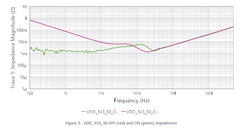
The stated requirement was to avoid sharp parallel resonances with a Q greater than 1.4 and to keep impedance below the target across the frequency range. For this rail, the target was approximately 8 mΩ through 7 kHz, then allowed to rise inductively at 20 dB per decade.
This target was based on a 5% voltage deviation and a 50 µs, 20.7 A current step. The reported measured impedance was below the target.
Why can the measured loadline differ from the regulator loadline?
The VDD_3V3_S0 regulator implemented a shallow 100 µΩ loadline, but the plot showed an apparent 2 mΩ loadline at the lowest frequencies. The stated reason is resistance between the probe location and the rail's remote-sense location.
Note: A measured low-frequency result can include resistance associated with the chosen probing point. The probe location therefore matters when interpreting a loadline.
Which other rails were measured with the same calibration?
The same calibration was used to measure VDD, a core-power rail below 1 V, near a multiphase current-mode voltage regulator. The ground-side pogo pins contacted ground copper around the inductors, while the power-side pins contacted the inductor outputs.
AVDD, another sub-1 V multiphase current-mode rail, was also measured near its selected location. AVDDH was measured near the inductor output and was identified as a single-phase voltage-mode buck rail.
| Rail | Description in the measurement | Observed interpretation |
|---|---|---|
| VDD | Core power below 1 V; multiphase current-mode regulator | Measured near the regulator using the same calibration |
| AVDD | Sub-1 V multiphase current-mode rail | Measured at its indicated probing location |
| AVDDH | Single-phase voltage-mode buck rail | No loadline capability; impedance decreased toward 0 Ω as frequency decreased |
What changes are needed for higher-frequency 2-port probe measurements?
Higher-frequency work with a high-frequency VNA requires the four pogo-pin tips to have identical deflection during calibration and measurement. Fully depressing all four pins for every calibration step and measurement is one stated way to maintain this condition.
The process also requires Short-Open-Load calibration on each port individually, followed by an isolation calibration for each port using 50 Ω resistors at the probe-tip ends. Isolation calibration corrects coupling between ports caused by mutual inductance, which is identified as the most significant high-frequency error source when its behavior differs between calibration and measurement.