New generations of chips with nanometer dimensions, high transistor density, and ultra-thin dielectric layers are making the problem much more difficult than before. Many failure mechanisms do not appear immediately but accumulate over time under the influence of electric fields, temperatures, or high current densities.
This is also why wafer-level reliability (WLR) testing systems are increasingly used in semiconductor research labs and modern chip technology development lines.
Why is the semiconductor industry gradually shifting towards on-wafer inspection?
Previously, many reliability tests were performed after the components were fully packaged. While still effective, this method was time-consuming, costly, and offered limited quick feedback if manufacturing errors occurred.
In contrast, direct wafer testing allows for much earlier detection of problems before the packaging stage.
WLR measurements enable engineers to:
- monitor transistor degradation
- assess dielectric strength
- analyze the effects of temperature and electric field
- predict component lifespan under real-world operating conditions
Thanks to faster data feedback, the process of optimizing technology is significantly more efficient, especially in semiconductor manufacturing lines developing new transistor structures or materials.
What types of failure mechanisms does WLR typically focus on?
One of the most important aspects of WLR is simulating stress conditions to observe how components change over time.
Tests often focus on common degradation mechanisms in transistors and metal-metal bonds.
The phenomenon of high-energy charged particles causing transistor degradation
Hot Carrier Injection (HCI) occurs when high-energy charge carriers are rapidly accelerated within the transistor and collide with the gate dielectric layer.
Over time, this process can lead to:
- a shift in threshold voltage
- a decrease in mutual conductivity
- changes in the transistor's operating characteristics
This is a crucial test for small transistors because the influence of electric fields in modern components is much greater than before.
Temperature instability and negative voltage across the PMOS transistor
Negative Bias Temperature Instability (NBTI) commonly occurs in PMOS transistors when operating at high temperatures under negative bias voltage for extended periods.
This phenomenon causes the transistor's electrical characteristics to gradually change over time, directly affecting the stability of the processor chip.
In newer semiconductor technologies, NBTI has become a mandatory test because the degradation rate is sometimes significantly faster than in older transistor generations.
High current can damage the metal bonds inside the chip
Electromigration (EM) is the phenomenon where metal atoms are gradually displaced due to excessively high current density.
When this process is prolonged, the metal conductors can:
- increase resistance
- form voids
- even break completely
This phenomenon is particularly noticeable in high-density chips or high-power components, where current is strongly concentrated in very small bonds.
Testing the durability of the dielectric layer over time
Time Dependent Dielectric Breakdown (TDDB) focuses on evaluating the durability of the gate dielectric layer under the influence of an electric field over a long period.
This test helps determine:
- the dielectric breakdown threshold
- the oxide layer degradation rate
- the long-term operating capability of the transistor
As the oxide layer becomes thinner in modern semiconductor technologies, TDDB has become an almost essential part of the evaluation process.
The 4200A-SCS system supports multiple measurements on a single platform
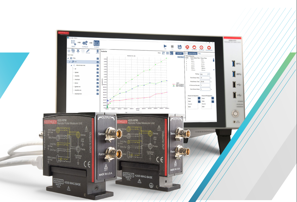
4200A-SCS is developed as a modular semiconductor parameter analysis system, allowing for various measurements on a single hardware platform.
The system can handle:
- Current-voltage measurements
- Capacitance-voltage measurements
- High-speed pulse measurements
Convenience is that users do not need to change configurations significantly when switching between different measurement tasks.
In applications involving small transistors or extremely low leakage currents, the system also utilizes high-resolution measurement sources combined with noise filters to maintain more stable data across very low signal ranges.
The 4225 PMU module helps process very high-speed pulse measurements
A major challenge in measurements like NBTI is that components can recover very quickly after stress is removed.
If the measurement speed is not fast enough, the data obtained will no longer accurately reflect the component's state at the moment of stress.
The 4225 PMU module was developed to address this problem by enabling pulse generation and measurement at microsecond speeds.
The system also incorporates a 4225 RPM remote amplifier, which helps to:
- Switching between high-precision measurement and high-speed pulse measurement
- Minimizing changes to the connection scheme
- Reducing the effects of parasitic capacitance on the cable
Placing the amplifier close to the measuring device also helps to stabilize the waveform and reduce signal distortion in high-speed measurements.
Clarius+ software supports the automation of many measurement steps
The system comes with Clarius+ software, which includes pre-built test libraries for:
+ HCI
+ NBTI
+ TDDB
This allows users to automate many steps in the Stress Measure process instead of manually setting up each individual measurement.
The software also integrates a Formulator tool to:
+ process raw data
+ calculate transistor parameters
+ quickly extract characteristic values after measurement
The system is scalable for large-scale wafer testing
In addition to single measurements, the 4200A-SCS can also be connected to a switching matrix to perform parallel stress testing on multiple different test structures directly on the wafer.
This scalability helps to:
+ increase testing speed
+ optimize lab uptime
+ better suit semiconductor research and development environments
As the number of structures to be tested on modern wafers increases, automation and system scalability have become crucial factors for today's advanced semiconductor research labs.