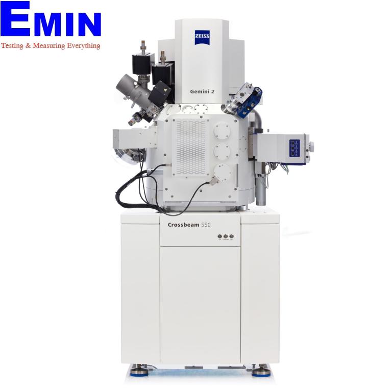
ZEISS Crossbeam 350 Electron Microscopy
Manufacturer: ZEISS Model: Crossbeam 350 Origin: Germany - Request a Quotation

- Request a Quotation
- Contact
See more: Equipment Calibration-Inspection & Repair Service
Call for the best priceHanoi city: (024) 35.381.269
Danang city: (023) 63.747.711
Bac Ninh city: (0222)730.39.68
HCM city: (028) 38.119.636
SEM Schottky Emitter:
1.7 nm @ 1 kV
1.5 nm @ 1 kV with Tandem decel
1.9 nm @ 200 V with Tandem decel
0.9 nm @ 15 kV
0.7 nm @ 30 kV (STEM mode)
2.3 nm @ 1 kV (WD 5 mm)
1.7 nm @ 1 kV with Tandem decel (WD 5 mm)
1.1 nm @ 15kV (WD 5 mm)
2.3 nm @20 kV & 10 nA (WD 5 mm)
Beam current: 5 pA – 100 nA
Store Resolution: 32 k × 24 k (up to 50 k × 40 k with optional Atlas 5 3D Tomography module)
Detection Limit: < 4,2 ppm boron in silicon
Lateral Resolution: < 35 nm
Mass/Charge Range: 1-500 Th
Mass Resolution: m/Δm > 500 FWTM
Depth Resolution: < 20nm AlAs/GaAs multilayer system
- Quality Engagement
- Easy change and return
- Delivery Avaliable
- Favorable payment